HKSTP and J2 Semiconductor Sign MoU to Promote the Development of Microelectronics Industry in Hong Kong J2 Semiconductor Plans to Establish R&D Center and First SiC Wafer Fab in Hong Kong
R&D Centre at Hong Kong Science Park under the plan will conduct independent R&D and production of third-generation semiconductor chips
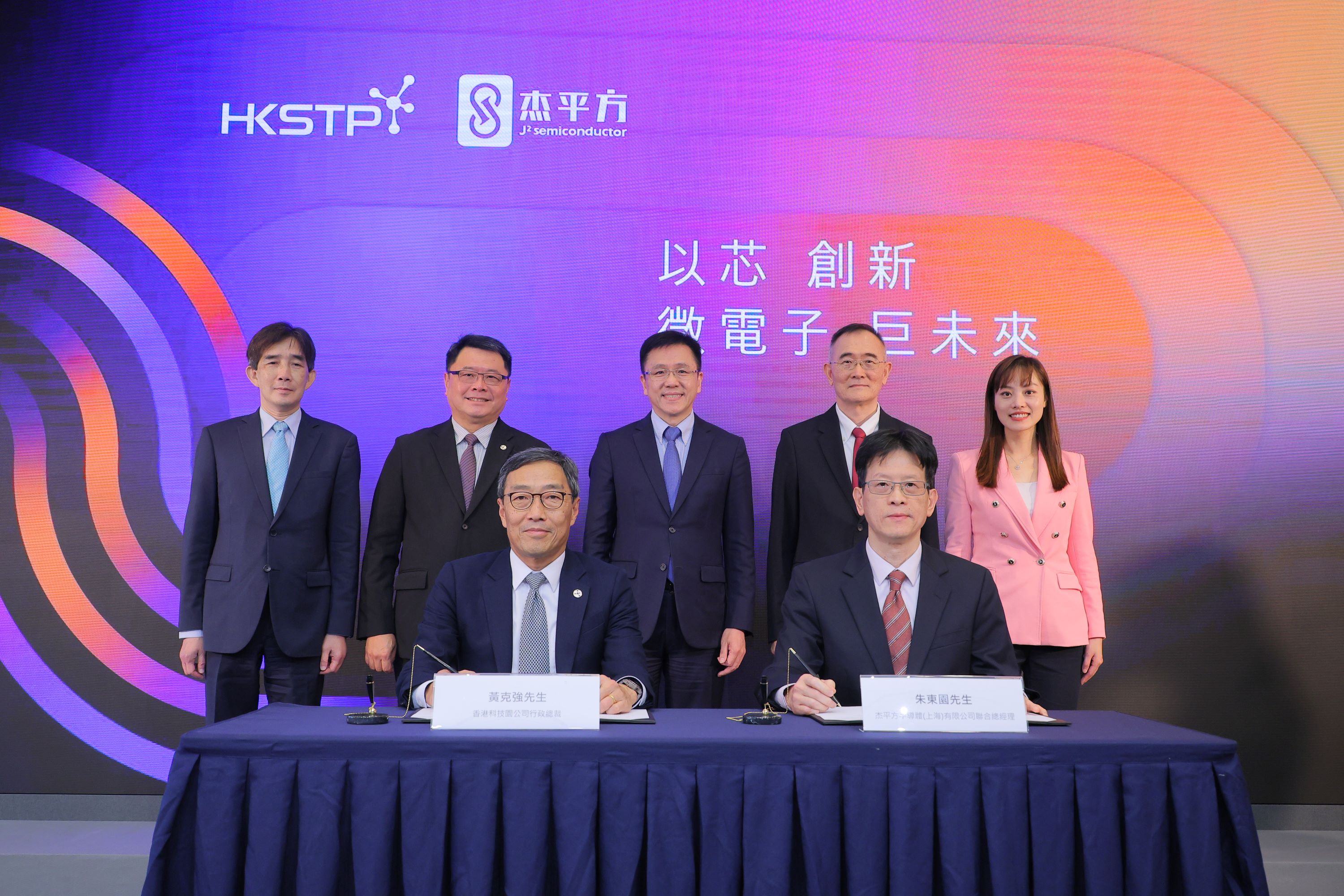
HONG KONG SAR - Media OutReach - 16 October 2023 - With support from the Innovation, Technology and Industry Bureau and the Office for Attracting Strategic Enterprises (OASES), the Hong Kong Science and Technology Parks Corporation (HKSTP) has signed a Memorandum of Understanding (MoU) with mainland China-based microelectronics enterprise J2 Semiconductor (Shanghai) Co.Ltd. (J2 Semiconductor), to set up a global research and development (R&D) Centre focusing on third-generation semiconductors at the Hong Kong Science Park, and to set up Hong Kong's first Silicon Carbide (SiC) 8-inch advanced wafer fab.

This is a milestone moment in the government's ambition to establish Hong Kong as a leading microelectronics hub in the region. This further promotes new industrialisation, a core for the Innovation, Technology and Industry Bureau which published its "Hong Kong Innovation and Technology Development Blueprint", with a mission to develop strategically advanced manufacturing industries, such as microelectronics and semiconductors. As one of the world's largest import and export markets for semiconductors, Hong Kong is at the heart of the Greater Bay Area which offers huge potential in becoming a key hub in the global semiconductor supply and value chain.
Professor Sun Dong, Secretary for Innovation, Technology and Industry, said "This collaboration between HKSTP and J2 Semiconductor to set up the Hong Kong's first-ever large-scale semiconductor wafer fab, demonstrates the commitment of the HKSAR Government in taking the initiative to turn its 'new industrialisation' vision into action. J2 Semiconductor is proactively building up the capacity, quality and competitiveness of Hong Kong's tech talent pool. The project will also drive the development of related industries, including semiconductor equipment manufacturers, material suppliers, testing service providers, to develop a complete ecosystem to reinforce Hong Kong's position in the global semiconductor industry value chain."
The collaboration between HKSTP and J2 Semiconductor is jointly supported by the Innovation, Technology and Industry Bureau and OASES with a view to sustain Hong Kong's innovation and technology ecosystem and promote new industrialisation. The MoU was witnessed by Professor Sun Dong, Secretary of Innovation, Technology and Industry Bureau, Mr Philip Yung, Director-General of OASES, Ms Lillian Cheong, Under Secretary for Innovation, Technology and Industry, Dr Sunny Chai, Chairman of HKSTP and Dr Robert Tsu, Chairman of J2 Semiconductor. While Mr Albert Wong, CEO of HKSTP and Mr TY Chu, Co-CEO of J2 Semiconductor formally signed the MoU.
Dr Sunny Chai, Chairman of HKSTP said, "The plan of establishing J2 Semiconductor's R&D Centre in the Science Park will promote Hong Kong's R&D and advanced manufacturing capabilities of third-generation semiconductor devices. J2 Semiconductor brings the core technology and expertise to Hong Kong in advanced chip design, fabrication process and semiconductor product development, which is an important milestone in the development of microelectronics industry in Hong Kong. As one of Hong Kong's flagship innovation and technology platforms, we provide high-quality infrastructure and facilities as well as a vast network of partners, which will continue to promote Hong Kong's microelectronics R&D capabilities and strengthen Hong Kong's position as an international I&T hub."
Dr Robert Tsu, Chairman of J2 Semiconductor said, "I am very grateful for the level of attention and support from both the Innovation, Technology and Industry Bureau and HKSTP to this project. The MoU signing officially launches our third-generation semiconductor 'SiC 8-inch advanced wafer fab' project. J2 Semiconductor will invest an estimated HK$6.9 billion into the project, with plans to start volume production in the next couple of years, and reach annual production capacity of 240,000 SiC wafers in 2028, generating an annual production value of more than HK$11 billion and creating more than 700 job positions in Hong Kong. The project will assist in the early completion of the localisation of the new energy vehicle supply chain and drive the long-term development and prosperity of the semiconductor industry in Hong Kong."
As a semiconductor chip design enterprise, J2 Semiconductor is committed to meeting the strong demand for domestically produced automotive chips from the China automotive industry. It mainly provides high-performance silicon carbide (SiC) devices with a focus on automotive, power conversion and communications. J2 Semiconductor's superior SiC technology can be applied to relevant applications such as electric vehicles, as well as the related infrastructure such as charging stations, smart grids and energy storage.
HKSTP is committed to promoting Hong Kong's new industrialisation mission and building a world-leading microelectronics ecosystem. HKSTP has established an extensive network of microelectronics hardware infrastructure, including Sensor Packaging and Integration Laboratory (Sensor Lab), Heterogenous Integration Lab (HI Lab) and the Hardware Lab, which can support the end-to-end process of design, prototyping and pilot production of chip-related equipment and systems as well as products. The Microelectronics Centre in Yuen Long Innovation Park is set to begin operation in 2024, supporting HKSTP's infrastructure to accelerate microelectronics R&D pilot production, creating opportunities for upstream and downstream enterprises in the industry chain.
The microelectronics ecosystem of HKSTP is flourishing, with more than 200 microelectronics related companies. The establishment of the J2 Semiconductor facilities in Hong Kong will create greater level of synergy and knowledge exchange. Currently, five universities in Hong Kong are ranked among the top 100 universities in the world, with more than 100 university researchers engaged in microelectronics research, and promote the R&D of third-generation semiconductors. In this year's Budget Speech, the HKSAR Government announced its plan to establish a Microelectronics Research and Development Institute to strengthen collaboration with universities, R&D centres and companies in the industry, and further accelerate the "1 to N" translation of R&D outcomes and bolster industry development.
Hashtag: #HKSTP
The issuer is solely responsible for the content of this announcement.
About Hong Kong Science and Technology Parks Corporation
Hong Kong Science and Technology Parks Corporation (HKSTP) has for over 20 years committed to building up Hong Kong as an international innovation and technology hub to propel success for local and global pioneers today and tomorrow. HKSTP has established a thriving I&T ecosystem that supported over 10 unicorns and Hong Kong's leading R&D hub with over 13,000 research professionals and over 1,400 technology companies focused on healthtech, AI and robotics, fintech and smart city technologies.
Established in 2001, we attract and nurture talent, accelerate and commercialise innovation and technology for entrepreneurs on their journey of growth. Our growing innovation ecosystem is built around our key locations of Hong Kong Science Park in Shatin, InnoCentre in Kowloon Tong and three modern InnoParks in Tai Po, Tseung Kwan O and Yuen Long. The three InnoParks are realising a vision of new industrialisation for Hong Kong. The goal is sectors like advanced manufacturing, electronics and biotechnology are being reimagined for a new generation of industry.
Through our infrastructure, services, expertise, and network of partnerships, HKSTP will help establish innovation and technology as a pillar of growth for Hong Kong, while reinforcing Hong Kong's international I&T hub status as a launchpad for growth at the heart of the GBA innovation powerhouse.
More information about HKSTP is available at www.hkstp.org.
About J² Semiconductor (Shanghai) Co. Ltd.
J² Semiconductor (Shanghai) Co., Ltd ("J2 Semiconductor") is a chip design company focusing on semiconductors for automotive and industrial applications. The company headquarters is currently located in Shanghai.
To meet the strong demand of worldwide automotive industry, especially in China, J² Semiconductor provides high-performance SiC devices, automotive signal chain ICs, and devices for the power conversion sectors. The company is actively expanding its product portfolio of automotive power devices, automotive signal chain chips, and automotive analog devices. The company also customizes products according to the customer needs, including high side drive (HSD), low side drive (LSD), half bridge drive (HBD), and DCDC synchronous buck converter.
J² Semiconductor has very solid management and technical teams with international and local background and experience, which enable seamless cooperation with customers in the automotive industry chain at home and abroad to deliver high-quality solutions. The company core team is well versed in circuit and device design, process development, high volume production, with strong understanding and know-how of automotive product requirement and qualification. With company principles of "Integrity, Innovation, and People-oriented", J² Semiconductor is committed to strive to become a world-class leader in the producer of third-generation semiconductor silicon carbide devices (IDM model).
J² Semiconductor has already secured funding and support agreement from a few top-tier investment organizations, renowned automotive and parts manufacturers.
More information about J² Semiconductor is available at www.j2semi.com.


